The Birth of the 74 Series
The 74 series ICs started back in the 1960s. Texas Instruments (TI) created these chips to help engineers build digital systems like computers and other gadgets more easily. The first ones were called the 5400 series, designed for military use—rugged and durable. Shortly after, the 7400 series came out for regular people and industries, offering similar features at a lower cost.

The 74 series chips were based on TTL technology (Transistor-Transistor Logic), which was fast and reliable at the time. As technology improved, the 74 series got better. New versions like 74LS (low-power) and 74S (high-speed) arrived in the 1970s and 1980s. Later, CMOS versions like 74HC chips appeared, using less power and working faster.
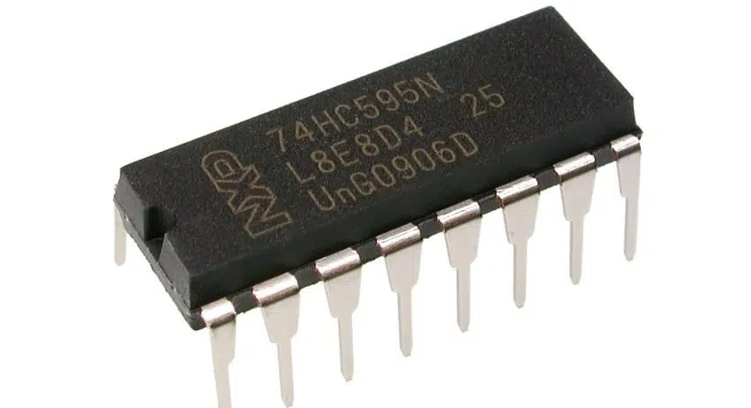
74HC595 Overview
The 74HC595 is an 8-bit shift register with a serial input, parallel output, and a built-in storage latch. It is commonly used in microcontroller projects to expand the number of output pins available, allowing you to control multiple devices like LEDs, displays, or other digital outputs using fewer pins on your microcontroller.
If your MCU is running low on output pins, the 74HC595 can come to the rescue. A shift register 74HC595 allows you to control 8 outputs using just 3 pins on a microcontroller.
Theoretically, you can link as many 74HC595 chips as needed using just 3 GPIO pins, because data is shifted serially through the chain. However, the more chips you add, the longer it takes to shift data through all of them. In practice, it’s common to chain 8 to 20 74HC595 chips. With 20 chips, you can control 160 outputs using just 3 GPIO pins on the MCU—that’s pretty amazing!
What is Shift Register
Understanding a shift register can be simplified with a real-world analogy. Think of it as a “conveyor belt” that moves items (data bits) step by step, and when the belt is full, you can pick all the items at once.
Serial Input
Imagine a row of 8 buckets on a conveyor belt. You place items (bits of data, e.g., 1 or 0) one at a time into the first bucket. When the conveyor moves, each bucket passes its item to the next bucket, making space for a new item.
Parallel Output
Once all the buckets are filled, you can see all 8 items at the same time (this is the “parallel output”). You can also decide to stop the conveyor temporarily to “freeze” and use the current state of items (using a latch).
Shift and Load
Shift
Every clock pulse moves the items in the buckets to the next position (like shifting a number). Example: Starting with 00000001, after 1 shift it becomes 00000010.
Load
When you’ve shifted all the data, you load (latch) the entire row to the output, which becomes visible to connected devices (e.g., LEDs).
74HC595 IC Pinout
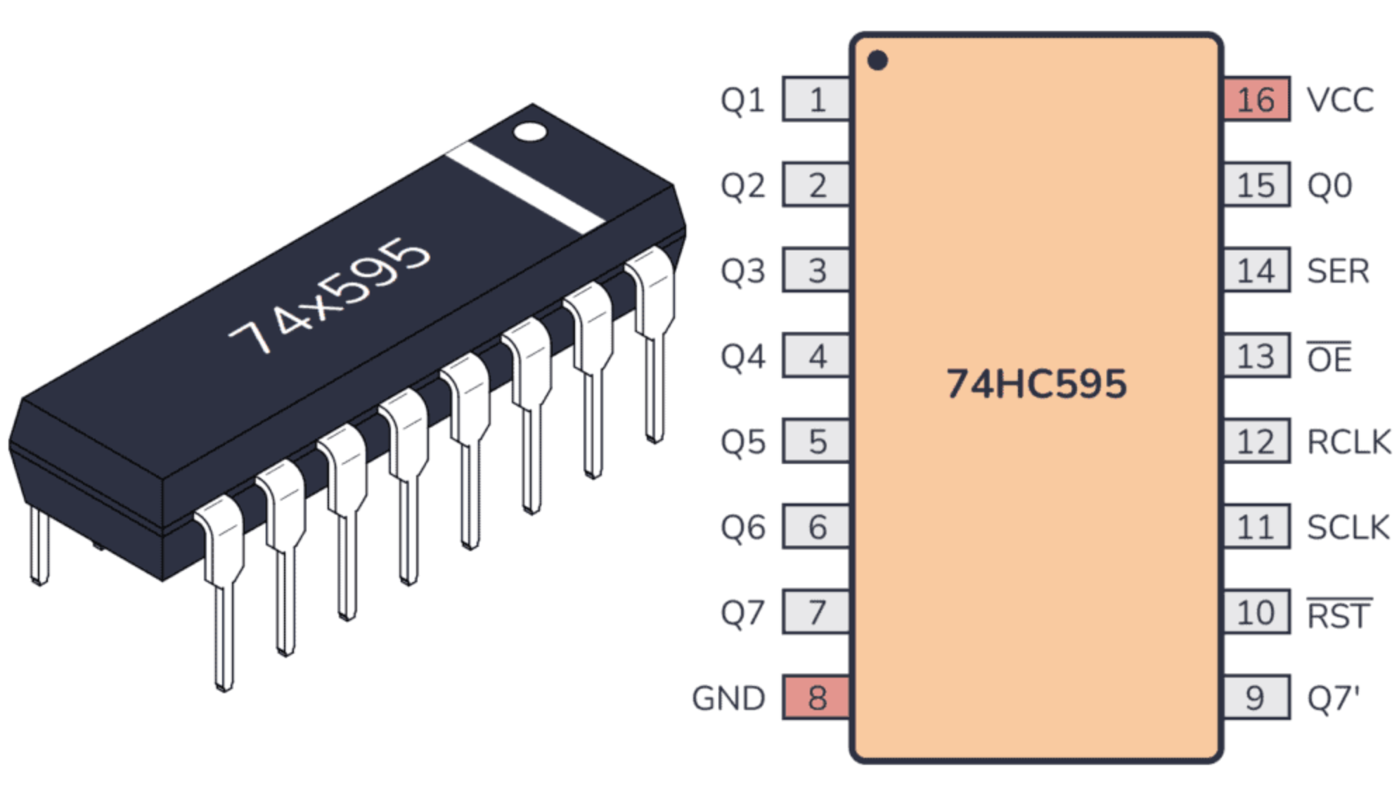
| Pin | Name | Function |
|---|---|---|
| 1 | Q1 | Output pin for bit 1. |
| 2 | Q2 | Output pin for bit 2. |
| 3 | Q3 | Output pin for bit 3. |
| 4 | Q4 | Output pin for bit 4. |
| 5 | Q5 | Output pin for bit 5. |
| 6 | Q6 | Output pin for bit 6. |
| 7 | Q7 | Output pin for bit 7. |
| 8 | GND | Ground |
| 9 | Q7′ |
Leave it if only have one 74HC595 Serial data output for cascading multiple shift registers. |
| 10 | RESET |
Connect to VCC Clears all outputs when pulled LOW. |
| 11 | SCLK (Clock) |
Shift Register Clock Pin. Data is shifted on the rising edge of this clock. |
| 12 | RCLK (Latch) |
Storage Register Clock Pin (Latch). Transfers the shifted data to the outputs on a rising edge. A rising edge is from LOW to HIGH. |
| 13 | OE (Enable) |
Connect to GND Enables or disables outputs when LOW or HIGH, respectively. |
| 14 | SER (Data In) |
Serial data input. The data to be shifted into the register is provided here. |
| 15 | Q0 | Output pin for bit 0. |
| 16 | VCC | Supply Voltage (3.3V or 5V) |


